
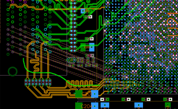
Manufacture of Printed Circuits from prototype to very large series
PCB-FAB’s production units allow us to meet all your needs, from the simplest printed circuits to the most technical PCBs.
- 1 to 42 diapers
- Rigides, flex et Flex-rigides stds et Multi-pressages
- Materials FR4 - HTG 170 ° -180 ° - flexible and rigid POLYIMIDE - High Frequencies: ROGERS, TEFLON etc…
- Finish: HAL SnPb, HAL Lead Free, chemical Sn, chemical and electrolytic NI / AU, OSP ...
- Substrate thickness: 0.1 to 8 mm
- Thick copper up to 435 µm
- Minimum tracks and insulation: 0.035 mm
- Minimum drilling: 75 µm by laser drilling and 150 µm in traditional
- Blind and buried holes (HDI circuits)
- Maximum panel size: 800 * 1200 mm (more on request)
- Controlled impedances: guaranteed up to + or - 5% with supply of the test coupon and measurement report.
- Saving varnish and screen printing: colors to choose from
- Peelable varnish

High Tech PCB
- Printed circuits HDI (High Density Interconnect)
- Via in pad (capped via)
- µvia Copper Filling
- Via bites with non-conductive paste, copper, sparing varnish or via SD-2361 “Peters” filler
- Stacked µvia
- Clean room class 1000 / 10,000 / 100,000 for complex cards
- Possibility of using different substrates on the same card thanks to the "laser adjustment" technology of our press
Our values
Easy and fast
Complete the form with or without your gerber files and our experts will analyze your request and send you a quote.
Trust
We have been working for more than 20 years in the field of PCBs for our European customers, we will solicit the best of them for the manufacturing.
Quality PCB
Each order is made with the greatest care and according to European Quality Standards CE or UL for the American standard.